MegaIO is a peripheral expander, based on an Atmel AVR microcontroller, designed to help processors that are short on I/O resources. MegaIO adds a UART (serial port), PWM outputs, A/D converter, and other features to to any processor or device capable of driving an I2C interface. MegaIO is quite functional but is still in development.
Common uses of MegaIO include:
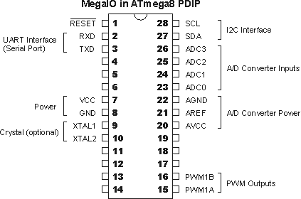
MegaIO was primarily designed to run on the ATmega8 processor from the Atmel AVR Series. Most of this document assumes the use of an ATmega8. Please note, however, that the MegaIO firmware can be adapted for use on any of the Mega processors in the Atmel AVR Series.
| Pins | Description |
RESET |
This pin can reset the MegaIO back to it's power-on defaults. For normal operation, connect RESET to VCC, preferably through a 10K resistor. Connect RESET to ground momentarily to reset the MegaIO. Note: Do not leave RESET unconnected, as this will result in erratic operation of the MegaIO. For advanced users, you can disable this pin by altering the processors fuse bits. |
RXD, TXD |
These two pins are the Receive Data and Transmit Data pins of the MegaIO UART (serial port). You can use these pins to talk to devices that operate over a serial port. Note that these pins are logic level only (Low=0V High=5V) and need an RS-232 level converter like the MAX232 chip before they can be connected to a serial port DB9 connector. |
VCC, GND |
These are the power pins for MegaIO and must be connected to a power supply voltage between 3-5VDC. MegaIO typically draws 2-5mA. |
XTAL1, XTAL2 |
These pins allow MegaIO to use a quartz crystal to improve timing accuracy or serial port baud rate accuracy. Crystal support is still in development. |
PWM1A, PWM1B |
When instructed to do so, MegaIO can produce PWM (pulse-width modulated) signals on these two pins. Duty cycle can range from 0-100% and several output frequencies are possible. |
AGND, AREF, AVCC |
These are the power supply pins for the analog-to-digital converter. For normal use, connect AGND and AVCC to the GND and VCC pins. Leave AREF unconnected. |
ADC0-3 |
These are the A/D converter input pins. Voltages of 0-AVCC can be read at these pins and converted to a number. Caution: Applying input voltages that exceed the range of 0-AVCC may damage the chip. |
SCL, SDA |
These are the I2C interface pins of MegaIO. These pins should be connected to your controlling processor's I2C SCL and SDA pins. |
The MegaIO module is commanded through an I2C bus interface. All commands and data reads/writes are sent through this I2C interface. I2C was developed by Philips Semiconductor and is a flexible bi-directional data bus which runs over just two wires. NOTE: I2C also goes by other names like TWI (two-wire interface) and SMBus (system management bus). In most cases, devices and controllers that use TWI or SMBus are completely compatible with each other and I2C.
Many microprocessors and microcontrollers have a built-in I2C interface. This includes products like the BasicStamp and the Mega line of Atmel AVR Series processors. For specific information about how to use the I2C interface on your microcontroller or system, see the datasheet or documentation that came with it. Once you're familiar with how to use I2C on your system, the information below should look familiar and make sense.
Interesting note: Nearly all modern PC motherboards use I2C (under the name SMBus) to control low-level functions like fan speeds and read CPU/motherboard temperatures. Although access to this SMBus is somewhat difficult under Windows, many Linux tools are available for accessing the bus.
For detailed information about the I2C protocol itself, see the I2C-bus specification at Philips Semiconductor.
The I2C standard specifies that all communications must have the following format:
| I2C Start | I2C address | R/W | Ack | Data0 | Ack | Data1 | Ack | ..... | DataN | NAck | I2C Stop |
7-bits |
1-bit | 1-bit |
8-bits | 1-bit | 8-bits | 1-bit | 8-bits | 1-bit |
The I2C address of the MegaIO is 0x4C hex or 0100110x binary (where 'x' is the R/W bit).
To write to a MegaIO register, send a standard I2C packet where the first data byte is the register number to be modified, and the remaining data bytes are the data to be written to that register. If you wish to select the register, but NOT change its value (write to it), then send only the register number and no data bytes. This is useful for performing a read operation (see below). *The Acks/Nacks have been left out for clarity.
| I2C Start | I2C address | W | Register | Data0 | ..... | DataN | I2C Stop |
1-byte |
1-byte |
1-byte | 1-byte | ||||
In order to read from a MegaIO register, you must first select it using an I2C write. After a register is selected, any subsequent I2C reads will read data from the selected register. *The Acks/Nacks have been left out for clarity.
| I2C Start | I2C address | W | Register | I2C Stop |
1-byte |
1-byte |
|||
| I2C Start | I2C address | R | Data0 | Data1 | ..... | DataN | I2C Stop |
1-byte |
1-byte |
1-byte | 1-byte | ||||
The table below provides a list of the currently supported registers, and a description of their function:
The default I2C address of the MegaIO
is 0x4C
hex or 0100110x binary (where 'x' is the R/W bit).
You can assign a new address by writing to the MegaIO I2CADDR register (see
below).
| Reg# (Hex) | Register Name | Number of bytes | Access Type |
Description |
General Registers |
||||
0x00 |
IDSTRING | 0-16 |
R |
Identification string of MegaIO device. Should read "MegaIO Vx.x" |
UART Registers |
||||
0x10 |
UARTDATA | 0-20 |
R/W |
Data written to this register will be sent out the MegaIO serial port. Data received by the MegaIO serial port can be retreived by reading this register. |
0x14 |
UARTBAUD | 4 |
R/W |
Serial port baud rate. Data format is a 32-bit number, written Low
byte first, High byte last. |
0x15 |
UARTBAUDSEL | 1 |
W |
Serial port baud rate selector. This is an alternative way to select
standard baudrate rates. Data format is an 8-bit number. |
0x18 |
UARTRXBUFBYTES | 1 |
R |
Number of bytes in the UART receive (RX) buffer. This is the number
of bytes waiting to be read from the UARTDATA register. Data format is
an 8-bit number. |
0x19 |
UARTTXBUFBYTES | 1 |
R |
Number of bytes in the UART transmit (TX) buffer. This is the number
of bytes, written to the UARTDATA register, that are waiting to be transmitted
out the serial port. Data format is an 8-bit number. |
PWM Registers |
||||
0x20 |
PWM1CTRL | 1 |
W |
Control register for PWM1 outputs. |
0x21 |
PWM1FREQ | 1 |
W |
Control register for PWM1 output frequency. |
0x24 |
PWM1ADUTY | 2 |
R/W |
PWM Channel 1A Duty Setting. |
0x25 |
PWM1BDUTY | 2 |
R/W |
PWM Channel 1B Duty Setting. |
A/D Converter Registers |
||||
0x30 |
ADCCTRL | 1 |
R/W |
A/D Converter Control Register |
0x31 |
ADCCHSEL | 1 |
R/W |
A/D Converter Channel Select Register |
0x32 |
ADCRESULT | 2 |
R |
A/D Conversion Result Register |
I/O Port Access Registers |
||||
0x43 0x44 0x45 |
PORTB |
1 |
R/W |
PORTB Registers |
0x46 0x47 0x48 |
PORTC |
1 |
R/W |
PORTC Registers |
0x49 0x4A 0x4B |
PORTD |
1 |
R/W |
PORTD Registers |
Direct I/O and Memory Access Registers
(advanced users) |
||||
0x80 |
DIRECTIO |
1-2* |
R/W |
Write/read directly to/from the processor's I/O space. |
0x81 |
DIRECTMEM |
2-3* |
R/W |
Write/read directly to/from the processor's RAM memory space. |
MegaIO Configuration Registers |
||||
0xF0 |
I2CADDR |
2-3 |
W |
Change MegaIO I2C address. |
0xF1 |
OSCCAL |
2 |
W |
Recalibrate the MegaIO internal oscillator. |
C code for AVR processors using AVRlib's i2c function library:
// include AVRlib I2C functions
#include "i2c.h"

#define MEGAIO_I2C_ADDR		0x4C

// write one byte to a MegaIO register
void megaioWriteReg(unsigned char regnum, unsigned char data)
{
	u08 packet[2];

	// construct I2c data packet
	//   first byte is register address
	//   next byte is the data that will be written to that register
	packet[0] = regnum;
	packet[1] = data;
	// send 2 bytes (register and data) to MegaIO
	i2cMasterSend(MEGAIO_I2C_ADDR, 2, packet);
}

// read one byte from a MegaIO register
unsigned char megaioReadReg(unsigned char regnum)
{
	unsigned char data;

	// first select the register by writing 1 byte (register)
	i2cMasterSend(MEGAIO_I2C_ADDR, 1, ®num);
	// then read 1 byte from the selected MegaIO register
	i2cMasterReceive(MEGAIO_I2C_ADDR, 1, &data);
	// return the results
	return data;
}

void testUart(void)
{
	// set MegaIO baud rate to 9600
	megaioWriteReg(0x15, 0x05);
	// send "hello!" using the MegaIO uart
	megaioWriteReg(0x10, 'h');
	megaioWriteReg(0x10, 'e');
	megaioWriteReg(0x10, 'l');
	megaioWriteReg(0x10, 'l');
	megaioWriteReg(0x10, 'o');
	megaioWriteReg(0x10, '!');
}

void testPWM(void)
{
	// turn on PWM and set for 8-bit resolution
	megaioWriteReg(0x20, 0x08);
	// set PWM frequency for mid-range
	megaioWriteReg(0x21, 0x03);
	// set PWM1A for 50% duty = 256*50% = 128
	megaioWriteReg(0x24, 128);
	// set PWM1B for 25% duty = 256*25% = 64
	megaioWriteReg(0x25, 64);
} |
----Download this example code---- |
For the Basic Stamp:
Coming Soon |
----Download this example code---- |