Spyglass UI Board Front
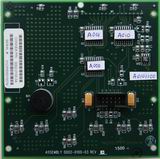
Spyglass UI Board Back
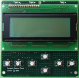
Spyglass UI Board Front |
Spyglass UI Board Back |
|
|
Spyglass UI Features:
Spyglass UI Pinout:
The pinout is shown looking into the connector on the back.
+5V |
Pin
1 |
X | X | 2 | +5V |
I2C SCL |
3 |
X |
X | 4 | GND |
I2C SDA |
5 |
X | X | 6 | GND |
NC |
7 |
X | X | 8 | Beeper +5V |
NC |
9 |
X | X | 10 | NC |
How to operate the Spyglass UI:
The Spyglass UI Board is controlled via three (3) PCF8574 I2C 8-bit I/O expanders, and one 8-bit I2C DAC. The parts are as used as follows:
Part |
I2C Address |
Function |
PCF8574 #1 |
0x40 |
Reading the pushbuttons |
PCF8574 #2 |
0x42 |
Controlling the LCD data lines DB0-7 |
PCF8574 #3 |
0x44 |
Controlling the LCD control signals RS, R/W,
E, and the LEDs and piezo beeper |
MAX518 DAC |
0x58 |
Controlling LCD Contrast |
Each PCF8574 has 8 I/O pins which can be read and written via the I2C bus. Here is how they are connected.
Part (I2C address) |
I/O pin # |
Function/Connection |
PCF8574 #1 (0x40) |
P0-6 |
Pushbuttons S1-7 |
|
P7 |
Not connected |
PCF8574 #2 (0x42) |
P0-7 |
LCD Data Lines DB0-7 |
PCF8574 #3 (0x44) |
P0 |
LED D2 |
|
P1 |
LED D3 |
|
P2 |
Beeper |
|
P3 |
Not connected |
|
P4 |
Not connected |
|
P5 |
LCD Control Line RS |
|
P6 |
LCD Control Line RW |
|
P7 |
LCD Control Line E |
- |
- |
- |
Datasheets for select parts:
Example source code: